· Products · 41 min read
STM32 Analog Slave
A dedicated analog input device with I2C and Modbus support
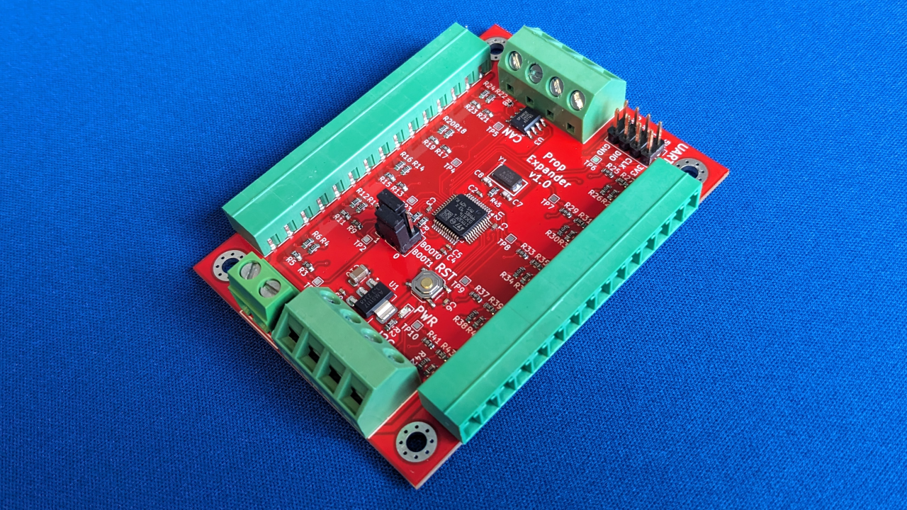
Every once in a while I end up requiring more IO for a prop than my boards have headers for. I’ve had “make an IO expander for your ecosystem” on the to-do list for a while, but due to time limitations I’ve always opted to grab prebuilt solutions to expand my IO, such as a MCP23017 board. Thanks to a recent commission and a sponsor from PCBWay, I pulled this out of the idea box and made it.
Choosing a Solution
Recently I had a client request a full escape room build. Multiple portions of the escape room require more IO than my current boards allow. In the past, I have also had use cases requiring several analog inputs, such as a large array of knock sensors. Looking at some of the solutions for dedicated SMD devices for analog, the price range for such chips ranged between $4-$12 and 4-8 analog inputs with a decent resolution.
Not liking those options, I turned to microcontrollers for their analog offerings. All of the microcontrollers I’m familiar with thus far are lackluster. The Arduino line has low resolution, the RP2040 also has low resolution, and the Espressif microcontrollers are “estimated” analog values and are the least accurate of them all. So, I dug deep into my plastic bin of “microcontrollers I vaguely remember using at one point”. Investigating and checking each board out of the bin, I landed on the notorious “Blue Pill” board.
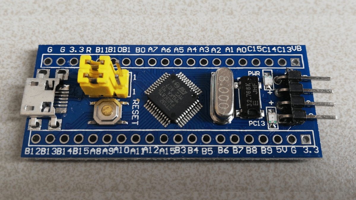
Small bit of history of the Blue Pill board if you’re curious:. The Blue Pill board is an STM32 microcontroller cloned from the original design of the Maple board by Leaflabs. This was the first board design from Leaflabs in 2009. An Arduino core was created to enable programming via Arduino IDE, and it immediately became a smash hit for hobbyists interested in transitioning from Arduino’s 8-bit architecture to a more modern 32-bit architecture. Suffering from its success, clones began to emerge from China at an incredibly low price point with a blue PCB and counterfeit components. However, with the Blue Pill board costing around $1.50 and working “with just a few issues”, it took off harder than the Maple boards. Even in 2024, these boards are still floating around while the Maple board retired in 2015.
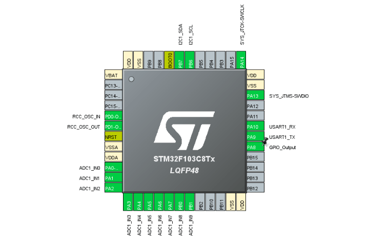
The microcontroller hosted on these boards is the STM32F103C8. Thanks to its popularity, it’s produced in high volumes and is extremely affordable at less than $1 per chip. In terms of features and performance today, it is an average microcontroller perfectly capable of handling any regular task. It’s capable of 12-bit analog resolution, which is pretty decent, and especially so for its price. There are two ADCs each with 10 channels, but they share the same pins, putting the microcontroller up to a total of 10 analog inputs (actually 15, but I’ll discuss that later). Board to board communication is possible with the device through I2C, UART, SPI, and CAN. It also supports DMA over analog, which means analog sampling can occur in the background without affecting the speed of the rest of the system.
The downside to choosing a microcontroller as an analog solution over a dedicated chip is development time. A dedicated IC needs less components compared to a microcontroller. Going even further, you can also buy fully complete solutions with no development required if you’re willing to pay for it. Also, significantly less programming is required to interface with a dedicated IC compared to a microcontroller. That extra couple of dollars you’ll spend on the dedicated IC may make up for the time, depending on your situation. My goal is to push down the hardware cost to a minimum to make replacements less impactful and to future-proof the idea of selling boards. Since I can program, design, and execute these solutions, I choose to develop it. This also gives me the freedom of deciding how it will operate.
Designing the PCB
In order to use the STM32F103C8 in a design, a few passive components are required. When working with analog, extra care must be taken in trace routing to reduce noise and interference in order to maintain accurate analog signals. There needs to be a way to program the board, interface with the board, and easily connect analog inputs as well.
Mandatory STM32 Components
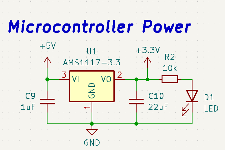
The board will be powered from an external 5V source, which will be stepped down with a 3.3V linear regulator. Decoupling capacitors were placed as close as possible to the power pins of both the microcontroller and the linear regulator. The shorter the distance between the path to the capacitors and power pins, the better they will perform in eliminating noise from the power circuitry.
An external oscillator is required to operate the microcontroller at its fastest speed of 72MHz. This is the noisiest component on the board and needs to be isolated properly to prevent its noise from affecting the analog inputs. ST has a good design guide for implementing oscillators in hardware. If you’re interested in eliminating noise from a circuit, even if you’re not designing a board for an STM32 microcontroller, the recommendations in this guide are applicable to any “isolate a noisy component” situation.
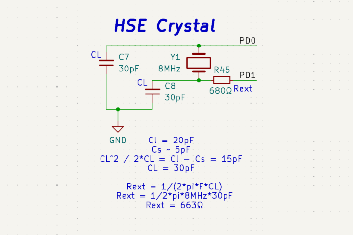
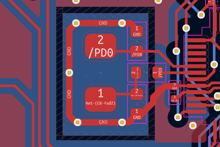
The oscillator must have an isolated ground plane separated from the rest of the board’s ground plane, and that ground plane must route directly to an available ground pin on the microcontroller. The recommended way to accomplish this per the design guide is to create a ground ring on the top layer of the board with vias connecting to the isolated ground plane on the bottom. This creates a barrier to catch oscillator noise permeating from the sides and route them into the ground plane instead of making their way to any sensitive signals. The ground plane is then routed to the nearest ground pin on the microcontroller with the shortest distance possible.
Programming Reset, and Boot
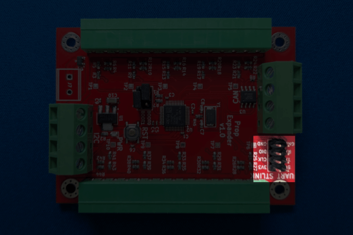
There are two ways to program the STM32F103C8: the standard JTAG header or a serial wire interface. Regardless of which method you choose, you’ll need an ST-Link adapter to program and debug the microcontroller. The serial wire interface requires less pins than JTAG, so I added the serial wire interface as standard pin headers, ignoring the JTAG interface.
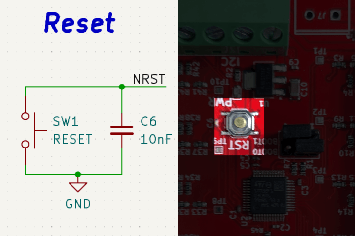
The reset pin is pulled up internally and is activated by pulling the pin to ground. A simple button and debouncing capacitor is utilized for hardware resetting.
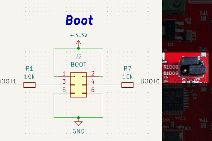
In order to flash the microcontroller, BOOT0 must be HIGH and BOOT1 must be LOW. To run the code, BOOT0 must be LOW. I didn’t want to be locked out of switching both the BOOT polarities in case I needed all the modes, so I mimicked the Blue Pill board and broke the BOOT pins out with standard header pins which are selected with a jumper.
Inputs
In my current prop board, I chose 3.81mm pluggable terminal blocks by mistake instead of 2.54mm terminal blocks. However, I’m now a fan of the slight size increase as it makes it easier to plug in cables without sacrificing too much board space. Going along with that preference, I chose the same type of terminal block for this board. Terminal blocks for wire connections are not the most cost efficient, but streamlining wire to board connections is essential for setting up and servicing electronics quickly on a work site, so I don’t compromise on it.
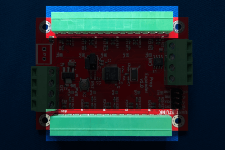
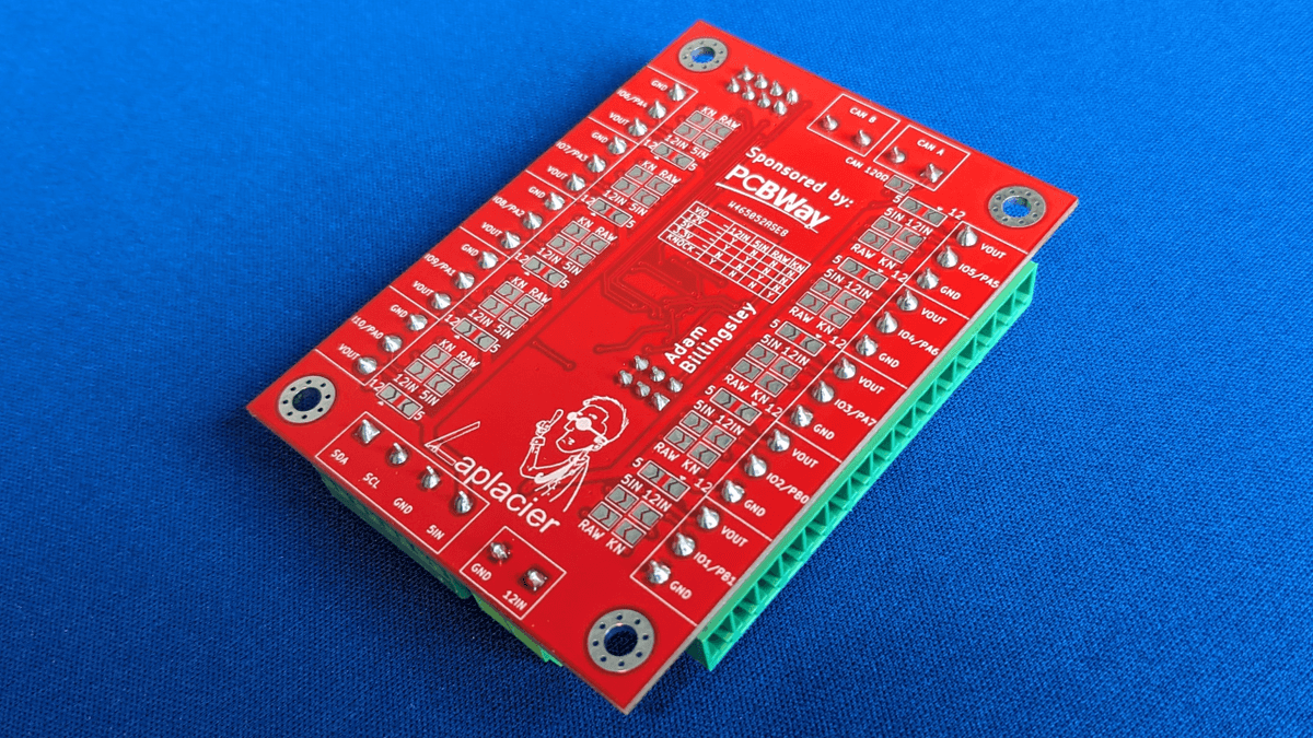
You won’t know ahead of time whether you’ll need power, ground or both for sensors interfacing with any given board. Sensors also utilize varying voltages. There are a lot of sensors out there, and each one has its own requirements. It’s impossible to account for all of them in a cost effective manner, but we can account for most of them by being compatible with 3.3V, 5V, and 12V. Each input has a resistor network selectable by solder jumpers depending on whether these 3 voltage levels are being delivered by the connected sensor.
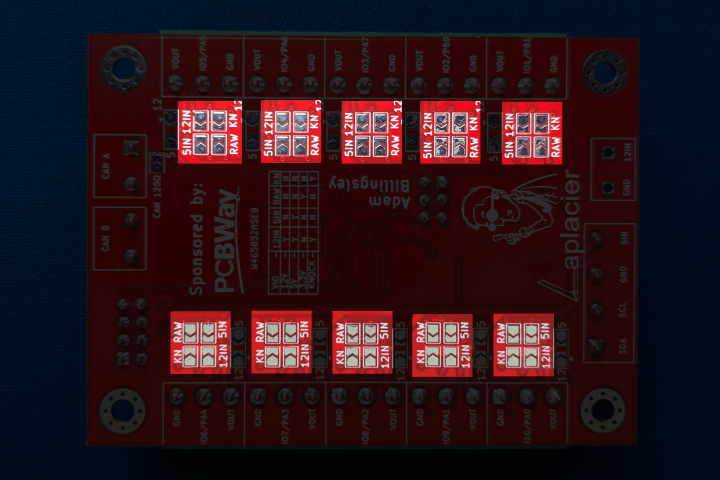
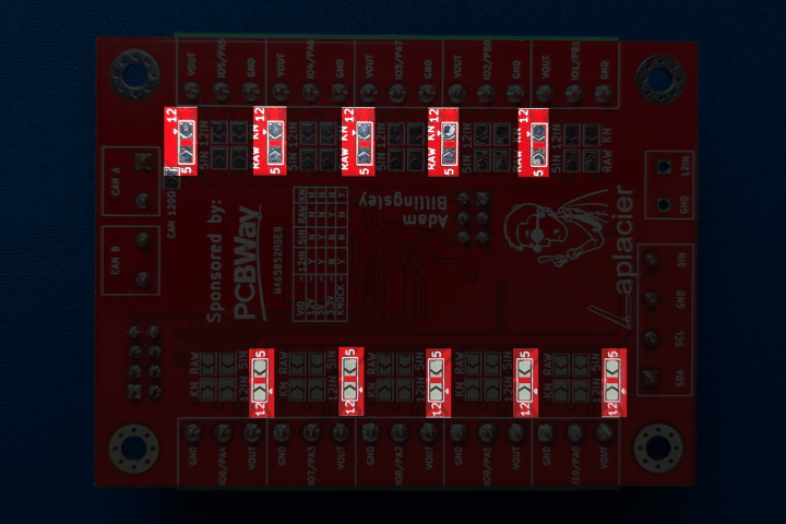
Each input also sports a solder jumper for delivering 5V or 12V power to the sensor and a ground. If the sensor is 3.3V, the resistor network can be completely bypassed with another solder jumper, which sends the signal directly to the microcontroller. To keep track of the jumpers, I added a table on the back as a guide to choose which jumpers to solder for a given voltage.
Communication
Since this board’s purpose is to receive input data from its input pins to send to other devices, it functions as a slave device. In the niche case where I need to implement more than 10 additional analog inputs, multiple boards should be able to communicate through the same wire. I initially decided on I2C and CAN. I2C is an extremely common method for hobbyists to interface with sensors and peripherals, so this protocol makes sense for myself and others to use.
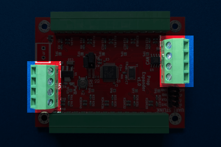
I also wanted a protocol that allows long distance communication in case a longer cable is necessary, so I initially chose the CAN protocol. However, between CAN and RS485, the latter made more sense for my application and the switch was made after the board was nearly finished. CAN is a masterless protocol where every device is free to communicate over the bus as long as space is provided. However, this board will exclusively behave as a slave device and will have no interest in behaving as a master. With RS485, I can implement the Modbus standard, which is a standardized and accepted method of transmitting data between one master and multiple slaves over an RS485 bus. Modbus is purpose-built for my application, and adopting it enables industrial controllers, PLCs, and computers with an RS485 adapter to interface with it.
In an effort to not lose it, I also added a UART breakout accessible via basic header pins. Adding a USB serial interface is less useful for STM32 since programming isn’t possible over UART. Implementing UART over USB also increases cost. With the header pin breakout, however, a serial adapter can be utilized.
Ordering via PCBWay
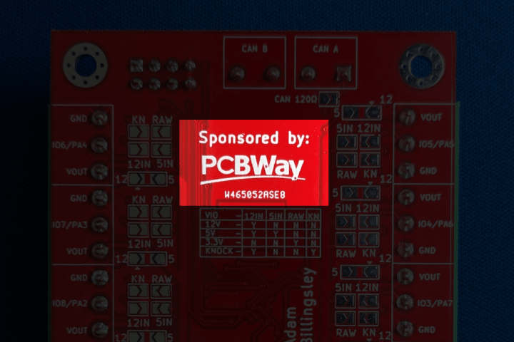
PCBWay sponsored the cost of the board, which allowed it to leave the idea phase and land on my workbench. In exchange, I’ll review my experience ordering an assembled board from PCBWay. Though they didn’t request it, I also added their logo on the bottom of the board as recognition of their offer.
Board fabrication
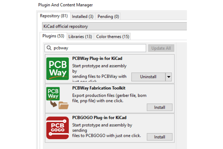
I designed my board through KiCAD 8.0, and PCBWay has an addon available for KiCAD that automatically exports a gerber with settings appropriate for their factory and pushes it to their order page with a click of a button. This is much faster than tediously cross referencing a manufacturer’s capabilities page and manually inputting gerber formats, specifying tolerances, and whatnot. Other than selecting cosmetic options on the ordering page, you’re good to go.
Speaking of cosmetic options, one thing I enjoy about PCBWay compared to other manufacturers I use is that 7 out of 10 of their solder mask colors do not incur an additional fee. I’m used to the price increasing when switching from the default FR-4 green color of PCBs. Thanks to that, I was able to make this board a red PCB guilt free.
While not utilized in the design, I noticed PCBWay is offering multi-color UV printing. This is an offering I’ve seen cropping up recently where you can have a color image applied to the top and/or bottom of your PCB via a UV printer. I have a backlog of ideas to implement for props with exposed PCBs, and this will enable a lot of creative liberty in those designs.
The pricing for the various options is more than reasonable for board fabrication. Board size matters when ordering in quantity. The STM32 Analog Slave board is 58.2x78.2mm, and I could choose up to 10 boards at a price point of $0.50 per board before addons. The next option, 15 boards, shoots up to $2.54 per board. Going up to the maximum quantity of board I’ve ever ordered, 100, the price settles back down to $0.77 per board.
This, however, doesn’t factor in the cost of shipping. Shipping 10 boards to my address costs $20.54 with DHL, while shipping 100 boards only increases shipping to $32.20. This brings the price point of 10 boards to $2.55 per board and 100 boards to $1.08 per board. As expected, buying in bulk saves money.
If you’re interested in a PCB made of aluminum instead of typical FR-4 and can squeeze your design into a single layer, it costs roughly the same as a two layer FR-4 board. Aluminum boards dissipate heat faster, allowing designs much more leeway when pumping lots of power through them. Don’t fabricate a 2+ layer board out of aluminum though, unless you’re planning to lose all your vacation money.
While it won’t matter to most hobbyists, FR-4 has different types that can resist heat better than others, which can help protect the board under extreme conditions or overexposure to a hot soldering iron. PCBWay automatically upgrades FR-4 to a strong type for free on 2-layer boards, and an even stronger type if your entire order is also larger than 3 square meters in area. I didn’t hit the 3 meter benchmark, but if you’re ordering in quantity this is a nice touch.
For board thickness, the standard is 1.6mm thick. Increasing the thickness past 1.6mm begins increasing the cost by a nontrivial amount. Decreasing the thickness reduces the price until 0.8mm, and lower than that begins to increase the cost again. I’m surprised 0.2mm thick boards are an option here, because I can’t imagine handling a board that thin. Nonetheless, I bet it has incredible applications for electronics in tight spaces.
Minimum track spacing is the same price between 4, 5, 6, and 8mil. If you drop your requirements down to 3mil minimum spacing, the price more than doubles. I played around with this and discovered that a 3.2mm thick board does not increase in price when dropping the minimum spacing to 3mil. If your design requires that tight spacing, take advantage of the thicker PCB.
Minimum via size can drop down to 0.25mm without a price change. 0.2mm bumped the price up by around 40%, and 0.15mm nearly tripled it. Luckily I’m not designing a board with a BGA chip where tiny vias are required to wiggle signals under and around the grid array.
Default silkscreen color changes based on the color of the solder mask you choose. If you choose a non-default silkscreen color, the price bumps up a little.
UV printing on one side is actually the same price as changing the color of the silkscreen. If you want to modify it, you might as well take advantage of this feature and apply a high quality decal on your board with the silkscreen as a part of the image. Applying a UV print to both sides barely increases the price compared to a single side, so have at it.
If your board has an edge connector, a surface finish of HASL with lead does not cost extra. If you want a gold finish for maximum conductivity, expect to sacrifice some bank balance for it. There are several more options between HASL and gold to offer a compromise between price and conductivity.
Vias are tented by default, and requesting them to be exposed does not increase cost. Plugging the vias completely with a solder mask increases the cost a small amount.
The copper thickness of the PCB layers can be increased if the minimum hole size is large enough. Smaller holes are unable to be drilled through thicker copper and stay within specification. The price increase per ounce of copper is fairly linear except for the change from 2 to 3 ounces and 11+ ounces. There is a significant jump at these values. Thicker copper means more power can be pushed through a thinner trace, which can help with squeezing power designs into a smaller footprint.
By default, PCBWay adds a product number to each board for identification purposes. You can remove it for a very small fee or specify a location on your board by adding WAYWAYWAY on the silkscreen of the board design where you want it. I recommend leaving the product number on the board as it helps when calling up the company with issues. Instead, place WAYWAYWAY on your board in a discreet location, like underneath a large component footprint. I placed mine directly under their sponsor logo as it made sense to do so.
Assembly service
While I’m capable of assembling my own SMD boards, it almost always makes more sense for me to take advantage of the manufacturer’s assembly service. Utilizing an assembly service is going to be more cost efficient than manually placing the components yourself if your board has more than 5-10 components to place on it. With PCBWay’s assembly pricing, this rule remains true. If you’re designing a board with assembly service in mind and want to reduce cost there are a few tips to keep in mind.
The KiCAD addon does not help with filling in assembly information. It does produce the required bill of materials for assembly and include it, but I found that the information populated by the addon was incorrect. Modifying KiCAD’s BOM properties didn’t change the addon’s behavior. PCBWay provides a good template as an example though, so creating one wasn’t too difficult.
You can have PCBWay source the parts in your BOM, ship them to PCBWay yourself, or mix it up. Unless it’s strictly necessary, I recommend letting PCBWay acquire the components. They’ll know what packaging options work best for their setup, and can take advantage of sourcing components from vendors closer to their location to your benefit.
If you placed all components on one side of the board, the assembly cost is the same. If components are placed on both sides, choosing a double-sided assembly bumped the assembly cost up by about 60% in my sample. That’s not too bad, considering the difficulty of assembling components on both sides increases significantly due to gravity. Surface tension can keep very small components secure when upside down during reflow, but otherwise extra means are necessary. It’s more than a 60% difficulty increase in my experience.
You can specify if there are components or parts on your board that require more sensitive handling than the default soldering process. Selecting this option does not affect the listed price, but I hypothesize the price is negotiated on a case by case basis in this regard.
PCBWay includes an option to accept alternative parts made in China. I selected this option and throughout the assembly process no parts were substituted. If they can source the parts you specified, they won’t do this. I attempted to provoke this option when speaking with the customer service rep handling my assembly order, and I’ll detail that exchange in the next section.
The labor cost of assembling a through hole component is more expensive than an SMD component. Barring the cost difference of equivalent components in SMD and through hole form factor, your options are:
- Through hole component, but omit it from the assembly list and assemble the through hole component yourself upon arrival.
- Through hole component, and they assemble it.
- SMD component, but omit it from the assembly list and assemble the SMD component yourself upon arrival.
- SMD component, and they assemble it.
Option 3 defeats the purpose of an assembly service, so that option is out. If you can find an equivalent SMD component, this is the best option. If you only have 1-2 through hole components with few pins, option 1 could be your best option. Otherwise, you’ll have to pay the additional cost with option 2.
With all options set to 0 or their minimum value, the assembly cost starts at $2.90 per board for 10 boards, drops to $1.40 per board at 20, increases to $1.80 per board at 50, and drops to $1.20 per board at 200. The final breakpoint occurs at 1000 boards at $0.50 per board. Even at the 10 board breakpoint, the price is extremely affordable in terms of assembly.
I’m unable to find a price sheet for assembling the various components on PCBWay, which makes planning around the price of a design difficult, but I was able to play around with numbers on the website to obtain a rough idea. I obtained these breakpoints with my board design inputted. I manually modified the unique parts and component type from 0-1, 1-2, etc. and observed the price change. The exact pricing I obtained may be unique to my board, quantity, order date, and other factors, but can serve as a baseline for others. For “difficult SMD components”, this includes BGA chips, components with 20+ pins, and components with tight pin spacing. The only component that passed this threshold on my board was the STM32F103C8 microcontroller, which has 48 pins and tight pin spacing.
- Basic SMD component - ~$0.253-0.279 per part per board
- Difficult SMD component - $0.760-0.761 per part per board
- Through hole component - $0.507 per part per board
Customer Service and Corrections
Throughout the assembly process I had a few back and forth emails with PCBWay. Some were related to the general process, and others were in relation to issues I injected intentionally and unintentionally.
There were some components on the board where the exact part used did not matter. I tested the alternative parts checkbox I selected earlier using these components. As long as the pin headers on my board were the standard 2.54mm pitch, they could come from any vendor as long as they worked. I added the pin headers into the bill of materials but omitted the part number when submitting the order to see if they would handle it. Unfortunately, the representative insisted on a part number and didn’t invoke the substitute. I assume this option leans toward parts they struggle to source rather than automatically filling in common parts.
I ended up mistakenly sending them a part number for pin headers with the wrong pitch when correcting this. They ordered the part, then informed me by email of my mistake and allowed me to correct this without extra charge. The cost of that mistake should have been on me for that, but they took it upon themselves to rectify the issue. I sincerely appreciated the forward-thinking customer service.
Once the boards were assembled, PCBWay replied with pictures of the boards assembled to confirm that orientation of components was correct. I’m used to other manufacturers charging for an additional confirmation and having to triple check that the orientations of polarized components I provided were correct. It appears PCBWay confirms with the customer as a part of the service at no charge, which is unexpected and appreciated. Nothing was incorrect or out of place, but it’s nice to know I have that extra security when ordering through them.
Delivery and Physical Inspection
Hitting the order button, going through the corrections and confirmations with PCBWay, and packing the boards took about 10 days. This was largely due to time zone differences, since PCBWay is in China and I’m going to bed as they open up. It’s no fault on their end; they replied as I closed up and I replied the next day when I woke up. In a standard assembly without error corrections, I would wager the process would take about 5 business days. Pretty standard turnaround for a small run.
PCBWay recommended that I ship through DHL. It was a slightly more expensive shipping option than the rest, but I chose it per their recommendation. Packing the boards, shipping through DHL, and delivery to my door took 3 days. Most of my deliveries from China and neighboring countries take 10-15 days on average, so 3 days is mind bogglingly quick. That package definitely traveled on an airline.
Upon opening the package, every board was enclosed in a Ziploc antistatic bag, and the box itself was sufficiently bubble wrapped. Each board was cleaned post assembly with no flux residue. All of the solder joints were solid, no pins were bridged together, and the through hole joints were textbook in shape. The I2C and RS485 terminal block headers were slightly misaligned on a few boards, but I was able to heat up the joints and push them straight.
On every board there were fingerprint smudges on both sides. You might think this is a criticism, but this is actually a good sign. This means a human handled and inspected this board instead of being directly tossed in the shipping box without a thought. I had silently assumed that PCBWay only inspected the one board they sent me images of, but based on the fingerprints I was mistaken. They also left me an extra unpopulated PCB in the box. This wasn’t a useful addition, but it’s nice to have a reference piece without the visual clutter of components in the way. I could see it used as a way to label a clear plastic container indicating what boards are inside if stuck to the front.
Programming
I had two options to choose from to program the board: the manufacturer’s official toolchain with STM32CubeIDE, or the STM32 Arduino core with Arduino. I chose the manufacturer’s toolchain. While I have no experience using their toolchain, I enjoy how easy the hardware planning is with their project wizard. If there are any sort of limitations they’re automatically flagged in the project, such as UART2 and certain ADC1 channels not being able to activate at the same time or I2C preventing the use of system wake-up. I also wanted to get experience with their software in case I use more of their products at a later date, which is highly likely as I continue to develop boards.
Analog with DMA
By default, STM32CubeIDE generates code that initializes DMA and analog configurations when selected, but it does not start it. In order to do so, you need an array with enough space to store the values read via the analog inputs.
Once started, a DMA interrupt function in a file called stm32f1xx_it.c is called when the analog values are finished being read. I set the DMA to circular mode in the project wizard, so this continues indefinitely, calling the interrupt at the end of each cycle. It’s best practice to not put any heavy operations inside an interrupt function, so I simply set a flag to indicate that the ADC has finished a full read.
void DMA1_Channel1_IRQHandler(void)
{
  /* USER CODE BEGIN DMA1_Channel1_IRQn 0 */

  /* USER CODE END DMA1_Channel1_IRQn 0 */
  HAL_DMA_IRQHandler(&hdma_adc1);
  /* USER CODE BEGIN DMA1_Channel1_IRQn 1 */
  flag_adc_ready = 1;
  /* USER CODE END DMA1_Channel1_IRQn 1 */
}
In the main loop, the flag is checked. If the flag is raised, the data is stored, and the flag is lowered.
while(1)
{
  if(flag_adc_ready)
  {
    flag_adc_ready = 0;
    for(int i=0; i<10; i++)
    {
      /*
       * Write analog vals to input registers
       */
      modbus_input_reg[i] = (uint16_t)analog_buf[i];
    }
  }
}
Analog to Digital
Since it’s easy to do so, I also implemented an analog threshold value roughly half of the maximum analog value. With this, I can plug in boolean inputs, such as buttons or switches, and utilize them with the same board. This board is a bit overkill for the purposes of identifying boolean inputs, but I could have scenarios where I need additional analog inputs as well as boolean inputs. Having one board handle both will reduce build complexity.
while(1)
{
  if(flag_adc_ready)
  {
    flag_adc_ready = 0;
    for(int i=0; i<10; i++)
    {
      /*
      * Write digital vals to input states
      */
      if(analog_buf[i] > modbus_holding_reg[MODBUS_IO1_THRESH + i])
      {
        modbus_input[0] |= (uint16_t)(1 << i);
      }
      else
      {
        modbus_input[0] &= (uint16_t)(1 << i) ^ 0xFFFF;
      }
    }
  }
}
I2C with Interrupts
By default, STM32CubeIDE generates code that initializes I2C, but it does not enable the interrupts, so the appropriate function is added.
In order to act as an I2C slave, first we need to decide how it will communicate with a master requesting data. To get the board off the ground, I took the approach of command and value. The I2C request from the master will consist of:
- req[0] - The STM32 Analog Slave’s I2C address
- req[1] - A byte corresponding to the command for the slave to execute
- req[2] - A byte of additional information if required by the command
Each request will be a static size. If the master requests the value of an input pin, the last request byte will include the 0-index of the analog pin to send to the master.
In case the master needs to read the settings in the device, the last request byte will include the 0-index of the settings register to read.
static int i2c_rx_callback(void)
{
  int command = I2C_rxData[0]; // I2C command
  int val = I2C_rxData[1];  // Input# to act upon
  if (val>9)  // There are a total of 10 inputs (0-9)
  {
    // invalid input, clear and exit
    memset(I2C_rxData,'\0', I2C_RX_SIZE);
    // rxcount = 0;
    return 1;
  }

  switch(command)
  {
    case I2C_READ_VAL:
      I2C_txData[0] = (analog_buf[val] >> 8) & 0xFF;
      I2C_txData[1] = analog_buf[val] & 0xFF;
      break;
    case I2C_READ_CONFIG:
      I2C_txData[0] = (modbus_holding_reg[val] >> 8) & 0xFF;
      I2C_txData[1] = modbus_holding_reg[val] & 0xFF;
      break;
    case I2C_WRITE_CONFIG:
      // Unable to write in current structure
      break;
    default:
      return 1;
  }

  if(command == 255) // Reset MCU
  {
    HAL_NVIC_SystemReset();
  }
  return 0;  // success
}
Additional interrupt functions need to be populated for:
- I2C message reception is complete
- Completing reception of an I2C Rx byte
- Completing transmission of an I2C Tx byte
- A message received with the STM32 Analog Slave’s address
- An error occurring during I2C Rx/Tx
These are cookie cutter functions added to facilitate I2C communication, and are included in the code.
void HAL_I2C_ListenCpltCallback(I2C_HandleTypeDef *hi2c)
{
  HAL_I2C_EnableListen_IT(hi2c);
}

void HAL_I2C_AddrCallback(I2C_HandleTypeDef *hi2c, uint8_t TransferDirection, uint16_t AddrMatchCode)
{
  if(TransferDirection == I2C_DIRECTION_TRANSMIT)
  {
    memset(I2C_rxData,'\0',I2C_RX_SIZE);
    rxcount = 0;
    txcount = 0;
    HAL_I2C_Slave_Sequential_Receive_IT(hi2c, I2C_rxData+rxcount, 1, I2C_FIRST_FRAME);
  }
  else
  {
    rxcount = 0;
    txcount = 0;
    HAL_I2C_Slave_Sequential_Transmit_IT(hi2c, I2C_txData+txcount, 1, I2C_FIRST_FRAME);
  }
}

void HAL_I2C_SlaveTxCpltCallback(I2C_HandleTypeDef *hi2c)
{
  txcount++;
  HAL_I2C_Slave_Seq_Transmit_IT(hi2c, I2C_txData+txcount, 1, I2C_NEXT_FRAME);
}

void HAL_I2C_SlaveRxCpltCallback(I2C_HandleTypeDef *hi2c)
{
  rxcount++;
  if(rxcount < I2C_RX_SIZE)
  {
    if(rxcount == I2C_RX_SIZE-1) // Last expected data byte
    {
      HAL_I2C_Slave_Seq_Receive_IT(hi2c, I2C_rxData+rxcount, 1, I2C_LAST_FRAME);
    }
    else // More data bytes
    {
      HAL_I2C_Slave_Seq_Receive_IT(hi2c, I2C_rxData+rxcount, 1, I2C_NEXT_FRAME);
    }
  }
  if(rxcount == I2C_RX_SIZE) // Process on expected stop pos
  {
    i2c_rx_callback();
  }
}

void HAL_I2C_ErrorCallback(I2C_HandleTypeDef *hi2c)
{
  uint32_t ret = HAL_I2C_GetError(hi2c);
  if(ret == 4)  // AF error
  {
    if(txcount == 0)  // error is while slave is receiving
    {
      i2c_rx_callback();
    }
    else // error while slave is transmitting
    {
      // Nothing to do here!
    }
  }

  else if(ret == 1)  // BERR Error
  {
    HAL_I2C_DeInit(hi2c);
    HAL_I2C_Init(hi2c);
    memset(I2C_rxData,'\0',I2C_RX_SIZE);  // reset the Rx buffer
    rxcount = 0;  // reset the count
  }

  HAL_I2C_EnableListen_IT(hi2c);
}
Modbus with Interrupts
In order to use modbus, UART needs to be enabled. By default, STM32CubeIDE generates code that initializes UART, and no additional functions are needed to enable the interrupts.
STM32 does not include a standard RS485 or modbus library by default, so I created functions to facilitate modbus communication. The proper procedures to implement modbus are outlined in this technical document on the modbus organization’s official website. In its most basic form, we need to implement the following:
- Variables to store and write data that mimic modbus registers, coils, and inputs
- Decide where data is stored, and document the locations for master drivers
- A function to accept and read a modbus message
- Functions to read and write modbus registers, coils, and inputs
- A function to send a modbus message, in response to a master
- An error handler function to handle incorrect messages and invalid parameters
Registers, Coils, and Inputs
Translating the definitions of these data types into our use case, we need to implement the following data types:
- Holding Register - Two byte, unsigned values in an array that are readable and writable. These are where our settings, info, and configuration will go.
- Input Register - Two byte, unsigned values in an array that are read only. Analog values read from the inputs are stored here.
- Coils - A one byte array that is readable and writable. Each bit in a coil byte represents a toggleable ON/OFF output. We don’t have any outputs on our board, but it can technically do so if the solder jumper on an input pin is set for 3.3V. I will implement this and leave it unused in case I need it in the future.
- Inputs - A one byte array that is read only. Each bit in an input byte represents a boolean input. With this, I can choose to read an analog pin’s data in boolean format depending on whether it passes the analog threshold, saving execution time on the master if a boolean state is needed.
For the holding registers, I implemented the following settings:
- Whether an input on the board is configured as input, output, or flick output. Again, not utilized, but laying the groundwork for later.
- Analog threshold value for each analog pin. I need to be able to tune each input individually. For example, in a setting where I use photoresistors to detect light or a laser, each photoresistor is going to vary slightly, and light is going to hit each resistor differently depending on orientation and position in a room.
- Milliseconds required to detect a boolean state change. If a sensor is teetering right on top of the analog threshold value or a boolean sensor is connected that triggers multiple times when pressed, we want to avoid firing off a state change several times in a few milliseconds. This is technically unnecessary since the modbus master is in control of how fast data is sent rather than the slave, but it might have an application down the road. Implemented, but unused.
- Milliseconds to leave a flick output on before turning it off. This is intended for locks and solenoids that power on momentarily to unlock, and are not intended to remain on. Not utilized, but implemented for later.
- Flags that are checked periodically to save and load the current configuration. Any writes to the registers are not saved on power down or reset. In order to save the registers, a save function will write the registers to flash memory, and the load function will copy the flash memory back into the registers. The flash memory is also loaded into the registers when the microcontroller is booting. This will be useful for tuning analog threshold values on the fly, and saving them when finished adjusting. This also gives me a way to modify the slave address without reflashing the board if I need to use more than one or the address conflicts with another device on the bus.
- A flag that is checked periodically to reset the board. You always need a way to remotely force a reset on your device if necessary.
No thorough planning is required for the coils and inputs. It makes sense to stick with the philosophy of index 0 representing physical input 0 and so on for organization and programming purposes.
The modbus documentation lists specific modbus controllers and their maximum available registers, coils, and inputs. My board is none of these controllers, therefore I need to set the maximums myself. I took a quick glance online at what regular users of modbus threw out as their understood maximum values and implemented these maximums. Per the modbus specification, I need to implement these in order to send error messages when invalid parameters are sent.
#define READ_COIL_STAT_MAX 200 // 200 coils
#define READ_INPUT_STAT_MAX 125 // 125 inputs
#define READ_HOLDING_REG_MAX 125 // 125 registers
#define READ_INPUT_REG_MAX 125 // 125 registers
#define FORCE_SINGLE_COIL_MAX 1 // 1 coil
#define PRESET_SINGLE_REG_MAX 1 // 1 register
#define READ_EXCEPT_STAT_MAX 8 // 8 coils
#define FORCE_MULT_COIL_MAX 200 // 200 coils
#define PRESET_MULT_REG_MAX 60 // 60 registers
Modbus Functions
Each modbus message is capped with a CRC16 value for error correction. These values, and an example function written in C to generate an appropriate CRC16 are located at the bottom of the modbus specification document. I ripped the example out directly and modified the data types to satisfy the STM32CubeIDE compiler.
static uint16_t CRC16(uint8_t *puchMsgg, uint16_t usDataLen)
{
  uint8_t uchCRCHi = 0xFF; /* high byte of CRC initialized */
  uint8_t uchCRCLo = 0xFF; /* low byte of CRC initialized */
  uint32_t uIndex; /* will index into CRC lookup table */
  while (usDataLen) /* pass through message buffer */
  {
    uIndex = uchCRCHi ^ *puchMsgg++; /* calculate the CRC */
    uchCRCHi = uchCRCLo ^ auchCRCHi[uIndex];
    uchCRCLo = auchCRCLo[uIndex];
    usDataLen--;
  }
  return (uchCRCHi << 8 | uchCRCLo);
}
To send a modbus message, the message first needs to be populated with data based on the command from the master. That information is then capped with the CRC16. The RS485 module is set to transmit mode by driving the direction pin HIGH. The modbus message is transmitted via the connected UART, and the RS485 module is returned to receive mode.
static void modbus_send_data(uint8_t *data, uint16_t size)
{
  uint16_t crc = CRC16(data, size);
  data[size] = crc & 0xFF;
  data[size+1] = (crc >> 8) & 0xFF;

  HAL_GPIO_WritePin(GPIOA, GPIO_PIN_8, GPIO_PIN_SET);
  HAL_UART_Transmit(&huart1, data, size+2, 1000);
  HAL_GPIO_WritePin(GPIOA, GPIO_PIN_8, GPIO_PIN_RESET);
}
The methods to read an input or holding register are the same with only a few substitutions, so they’re bundled together in the same function. We determine what register the master wants to start reading as well as how many registers it wants to read, starting at that register. If it attempts to access registers outside the maximum amount of registers, we send an error message instead. If the request is good, we create a payload containing our slave address, the original command, the byte length of the data and the data to send. The message is then sent.
uint8_t modbus_read_register(uint8_t reg_type)
{
  uint16_t startAddr = uart_rxData[3] | (uart_rxData[2] << 8); // starting reg to read
  uint16_t dataLen = uart_rxData[5] | (uart_rxData[4] << 8); // # of regs to read

  /*
   * Determine read type
   */
  uint16_t *modbus_reg = NULL;
  uint16_t max_size;
  switch(reg_type)
  {
    case READ_HOLDING_REG:
      modbus_reg = modbus_holding_reg;
      max_size = READ_HOLDING_REG_MAX;
      break;
    case READ_INPUT_REG:
      modbus_reg = modbus_input_reg;
      max_size = READ_INPUT_REG_MAX;
      break;
    default:
      return ILLEGAL_FUNCTION;
      break;
  }

  /*
   * Check message validity
   */
  if(!dataLen || dataLen > max_size)
  {
    modbus_exception(ILLEGAL_DATA_VAL);
    return ILLEGAL_DATA_VAL;
  }
  if(startAddr+dataLen-1 > max_size)
  {
    modbus_exception(ILLEGAL_DATA_ADDR);
    return ILLEGAL_DATA_ADDR;
  }

  /*
   * Load UART data
   */
  uint16_t uart_index = 3;
  uart_txData[0] = SLAVE_ADDR;
  uart_txData[1] = reg_type;
  uart_txData[2] = dataLen * 2;

  for(int i=0; i<dataLen; i++)
  {
    uart_txData[uart_index++] = (modbus_reg[startAddr] >> 8) & 0xFF;
    uart_txData[uart_index++] = modbus_reg[startAddr] & 0xFF;
    startAddr++;
  }
  modbus_send_data(uart_txData, uart_index);
  return 0;
}
Reading coils and inputs are also similar, and can be bundled in the same function. Coils and inputs are stored bit by bit rather than in words, so we need to extract the values from each bit of a byte. Otherwise, the payload is structured the same as when we read registers. Once we construct the payload, the message is sent.
uint8_t modbus_read_state(uint8_t reg_type)
{
  uint16_t startAddr = uart_rxData[3] | (uart_rxData[2] << 8); // starting reg to read
  uint16_t dataLen = uart_rxData[5] | (uart_rxData[4] << 8); // # of regs to read

  /*
   * Determine read type
   */
  uint8_t *modbus_reg = NULL;
  uint16_t max_size;
  switch(reg_type)
  {
    case READ_INPUT_STAT:
      modbus_reg = modbus_input;
      max_size = READ_INPUT_STAT_MAX;
      break;
    case READ_COIL_STAT:
      modbus_reg = modbus_coil;
      max_size = READ_COIL_STAT_MAX;
      break;
    default:
      return ILLEGAL_FUNCTION;
      break;
  }

  /*
   * Check message validity
   */
  if(!dataLen || dataLen > max_size)
  {
    modbus_exception(ILLEGAL_DATA_VAL);
    return ILLEGAL_DATA_VAL;
  }
  if(startAddr+dataLen-1 > max_size)
  {
    modbus_exception(ILLEGAL_DATA_ADDR);
    return ILLEGAL_DATA_ADDR;
  }

  /*
   * Load UART data
   */
  memset(uart_txData, 0, 256);
  uint16_t uart_index = 3;
  uart_txData[0] = SLAVE_ADDR;
  uart_txData[1] = reg_type;
  uart_txData[2] = (dataLen / 8) + ((dataLen % 8) ? 1 : 0);

  uint16_t data_byte = startAddr / 8;
  uint8_t data_bit = startAddr % 8;
  for(int i=0; i<dataLen; i++)
  {
    uart_txData[uart_index] |= ((modbus_reg[data_byte] >> data_bit) & 0x01) << (i % 8);
    data_bit++;
    if(i && !(i % 8)) // Loaded a full byte, increase uart index
    {
      uart_index++;
    }
    if(data_bit > 7) // At end of data byte, goto next byte
    {
      data_byte++;
      data_bit = 0;
    }
  }
  modbus_send_data(uart_txData, uart_index+1);

  return 0;
}
When writing a register, we need to check if the data being written to the register is valid in our board’s specifications. We wouldn’t want to write a value to an analog input threshold that is larger than 4095, the maximum possible value, for example. Therefore we create a function to pass in the values that fails and sends an error message if invalid.
uint8_t modbus_validate_register(uint16_t holding_reg, uint16_t value)
{
  if(holding_reg >= MODBUS_IO1_THRESH && holding_reg <= MODBUS_IO10_THRESH)
  {
    // Threshhold value cannot be 0 or exceed the maximum analog val
    if(!value || value >= ANALOG_MAX)
    {
      return ILLEGAL_DATA_VAL;
    }
    else
    {
      return 0;
    }
  }

  if(holding_reg >= MODBUS_SAVE && holding_reg < MODBUS_CONFIG_MAX)
  {
    // The only valid toggle for a flag is 1
    if(value != 1)
    {
      return ILLEGAL_DATA_VAL;
    }
    else
    {
      return 0;
    }
  }

  // Cannot access nonexistent configuration registers
  if(holding_reg >= MODBUS_CONFIG_MAX)
  {
    return ILLEGAL_DATA_ADDR;
  }

  // Accessing a valid register with no value restrictions
  return 0;
}
The number of registers to read is excluded from the master payload when writing to a single holding register since the size is constant. After validating the data, we write the provided value to the register, then echo the master payload without the values written to the master to represent a successful write.
uint8_t modbus_write_single_register(void)
{
  uint16_t regAddr = uart_rxData[3] | (uart_rxData[2] << 8); // reg to write

  /*
   * Check message validity
   */
  if(uart_rxData[1] != PRESET_SINGLE_REG)
  {
    modbus_exception(ILLEGAL_FUNCTION);
    return ILLEGAL_FUNCTION;
  }
  if(!regAddr || regAddr > READ_HOLDING_REG_MAX)
  {
    modbus_exception(ILLEGAL_DATA_VAL);
    return ILLEGAL_DATA_VAL;
  }

  /*
   * Write holding register
   */
  uint16_t value = (uart_rxData[4] << 8) | uart_rxData[5];
  uint8_t ret = modbus_validate_register(regAddr, value);
  if(ret)
  {
    modbus_exception(ret);
    return ret;
  }
  modbus_holding_reg[regAddr] = value;

  /*
   * Load UART data
   */
  for(int i=0; i<6; i++)
  {
    uart_txData[i] = uart_rxData[i];
  }
  modbus_send_data(uart_txData, 6);


  return 0;
}
Writing to multiple holding registers adds the number of registers to read back into the master payload, with a value to write for each register. We loop through the specified registers writing each value, then echo the master payload without the values written to the master to represent a successful write.
uint8_t modbus_write_multiple_register(void)
{
  uint16_t startAddr = uart_rxData[3] | (uart_rxData[2] << 8); // start reg to write
  uint16_t dataLen = uart_rxData[5] | (uart_rxData[4] << 8); // # of regs to write

  /*
   * Check message validity
   */
  if(uart_rxData[1] != PRESET_MULT_REG)
  {
    modbus_exception(ILLEGAL_FUNCTION);
    return ILLEGAL_FUNCTION;
  }
  if(!dataLen || dataLen > READ_HOLDING_REG_MAX)
  {
    modbus_exception(ILLEGAL_DATA_VAL);
    return ILLEGAL_DATA_VAL;
  }
  if(startAddr+dataLen-1 > READ_HOLDING_REG_MAX)
  {
    modbus_exception(ILLEGAL_DATA_ADDR);
    return ILLEGAL_DATA_ADDR;
  }

  /*
   * Write holding register
   */
  uint8_t uart_index = 7;
  for(int i=0; i<dataLen; i++)
  {
    uint16_t value = (uart_rxData[uart_index] << 8) | uart_rxData[uart_index+1];
    uint8_t ret = modbus_validate_register(startAddr, value);
    if(ret)
    {
      modbus_exception(ret);
      return ret;
    }
    modbus_holding_reg[startAddr++] = value;
    uart_index += 2;
  }

  /*
   * Load UART data
   */
  for(int i=0; i<6; i++)
  {
    uart_txData[i] = uart_rxData[i];
  }
  modbus_send_data(uart_txData, 6);
  return 0;
}
Saving Settings
Flash memory on the microcontroller is significantly more robust than RAM, and we don’t need to access this data with low latency, so we’ll store data in flash. Per the STM32F103C8 datasheet, there are 64 “pages” of flash memory each containing 1024 bytes of flash. When we program the microcontroller, by default, the executable program is stored starting at the start address until it is completely written.
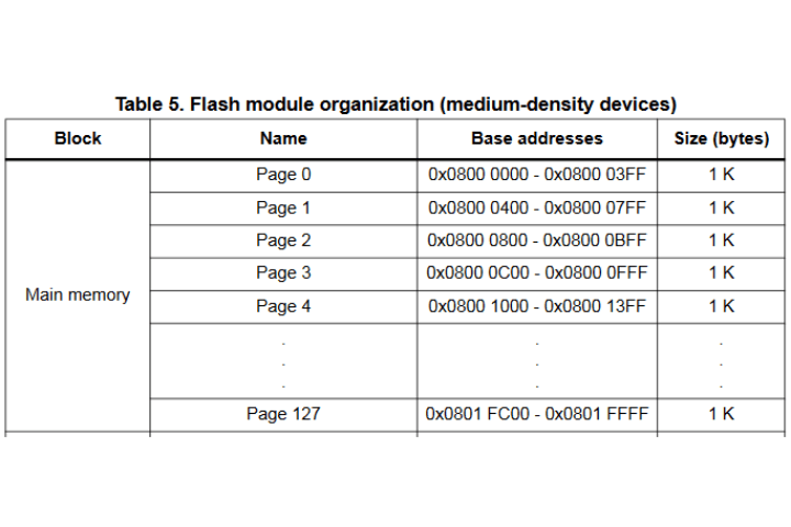
If we want to utilize flash to store data, we need to make sure we use data that isn’t in use by the executable. We want to store the data in the modbus holding registers, which contains a maximum of 250 bytes of data, so a single page of flash will suffice for storing data. To minimize the chance of touching the executable code, we’ll store values in the final page of flash.
To “load” modbus data, we need to copy the contents of the flash memory at the correct address to the modbus holding register variable. In case we’ve never saved data here before, we include default values to replace invalid ones.
uint32_t modbus_load_config(void)
{
  for(int i=0; i<MODBUS_CONFIG_MAX; i++)
  {
    modbus_holding_reg[i] = *(__IO uint16_t *)(FLASH_CONFIG_ADDR + (2*i));

    if(i >= MODBUS_IO1_THRESH && i <= MODBUS_IO10_THRESH)
    {
      if(!modbus_holding_reg[i] || modbus_holding_reg[i] > ANALOG_MAX)
      {
        modbus_holding_reg[i] = ANALOG_THRESHHOLD_DEFAULT;
      }
    }
  }
  return 0;
}
Saving modbus data by writing to flash memory requires some extra steps. First we need to unlock, or remove write protection, from the flash memory. As an additional failsafe, the HAL functions prevent programming nonzero flash memory, so we need to erase the memory first. Once erased, we can proceed to program flash one holding register at a time, then lock up the flash memory again to protect it.
uint32_t modbus_save_config(void)
{
  FLASH_EraseInitTypeDef EraseConfig;
  uint32_t ErrorIndex;
  uint32_t ErrorCode;
  EraseConfig.TypeErase = FLASH_TYPEERASE_PAGES;
  EraseConfig.PageAddress = FLASH_CONFIG_ADDR;
  EraseConfig.NbPages = 1; // Each page is 1024 bytes
  HAL_FLASH_Unlock();

  /*
   * Erase flash mem
   */
  if(HAL_FLASHEx_Erase(&EraseConfig, &ErrorIndex) != HAL_OK)
  {
    ErrorCode = HAL_FLASH_GetError();
    // Error code ErrorCode while erasing page ErrorIndex
    return ErrorCode;
  }

  /*
   * Write config to flash mem
   */
  for(int i=0; i<MODBUS_CONFIG_MAX; i++)
  {
    if(HAL_FLASH_Program(FLASH_TYPEPROGRAM_HALFWORD, FLASH_CONFIG_ADDR + (2*i), modbus_holding_reg[i]) != HAL_OK)
    {
      ErrorCode = HAL_FLASH_GetError();
      // Error code ErrorCode while writing address FLASH_CONFIG_ADDR + (2*i)
      return ErrorCode;
    }
  }

  HAL_FLASH_Lock();
  return 0;
}
Design Flaws
The most obvious design error on the board is CAN labeling on the board. The decision to transition from CAN communication to modbus was made before I put the design away, and when I returned to finish it I forgot about the transition and failed to check over everything properly. That left me with a board labeled and routed for CAN connected to an RS485 chip. Whoops! To make matters worse, the pins connected to the RS485 chip were incapable of transmitting UART data. I sacrificed the exposed UART interface, but I was able to route the correct pins over to the bus.
I mistakenly omitted the male portion of the pluggable terminal blocks and a 5.0mm terminal block header from the bill of materials, which resulted in them not being included with the order. Not much of a design flaw, but it did make testing the board more annoying.
I failed to put the recommended decoupling/power capacitors on the board for the STM32F103C8. In the early design phase I used the Blue Pill board as a template. As I began digging through the hardware design reference for this chip I slowly came to realize that the Blue Pill board added components where none were recommended, lacked most of the components that were recommended, and didn’t adhere to any of the noise reduction strategies. The Blue Pill is the perfect template for how not to design the board! I made all the recommended design changes in the manufacturer’s documentation, but somehow I missed the entire section about the power capacitors. This won’t harm the board, but by straying from the recommended decoupling array the analog inputs are likely a little noisier than they should be.
Specifically, the decoupling capacitors for the STMF103C8 should be five 100nF ceramic capacitors and one 10uF tantalum capacitor. Vbat should be connected to Vdd with a 100nF ceramic capacitor when unused, and Vdda should be decoupled with a 10nF ceramic capacitor and a 1uF tantalum capacitor.
I broke out BOOT0 and BOOT1 just like the Blue Pill board so I could alternate between flashing and executing the code on the microcontroller. However, as I discovered, the STLINK programmer can program the microcontroller while BOOT0 is left floating, which allows the code to be executed and flashed without touching anything. Turns out the counterfeit chips are lacking some proprietary data to allow that to happen, making the BOOT selectors mandatory. I ended up never needing to touch the jumpers, so they can be omitted.
Closing Remarks
There are a few flaws to correct on this design, but with the small batch I have I can still use them as intended with a bit of post processing. The last thing to complete is a driver on my prop boards to interface with the STM32 Analog Slave. I’ll use the I2C for now, since the current version of the prop board is not equipped with an RS485 chip. That will have to wait until the next revision.
I haven’t designed and printed a case for the board. I have a few modifications I may make to the layout, and I don’t want to invest time into a case design for a board that has only 10 copies. In the meantime, I’ll insulate the backside when installing them.
There will be some tweaking and fine tuning of the code over time as bugs arise. If I get the software and hardware into a comfortable state, I might replace the solder jumpers into more user-friendly circuits and sell these since they would have a very broad and effective use case.
Thanks again to PCBWay for covering the production costs! Without it, the board design would have been collecting virtual dust for a much longer time.